Introducing an initiative by WOW Alliance for the development of 3D integrated technology for LSI
Zuken is currently collaborating with Professor Takayuki Ohba Laboratory for Research of Science and Technology, Tokyo Institute of Technology, to participate in the WOW Alliance, an industry-academia research platform for research and development of next-generation semiconductors, as a joint effort to develop original 3D integrated technology for LSI.
Semiconductor development is said to have reached the limit with regards to the degree of integration that can be achieved through miniaturization. However, future expectations for 3D mounting technology, in which chips are mounted by vertical stacking, are high. WOW Alliance is currently developing new chiplet integration technology to solve challenges in 3D integration, such as reduced power consumption and thermal resistance, while improving performance at the same time.
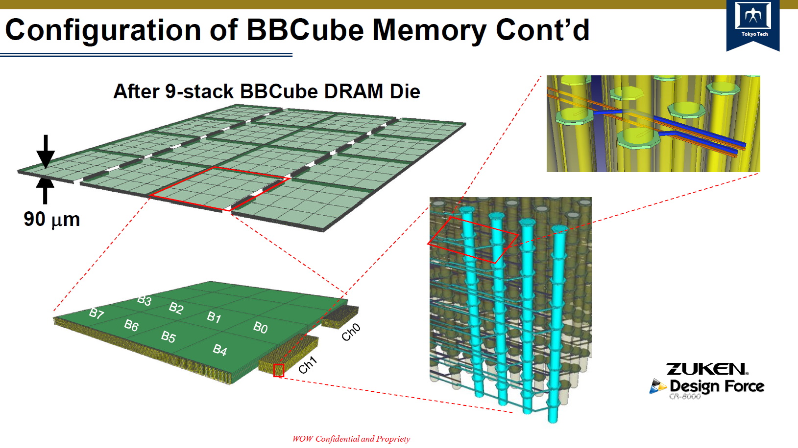
Within the WOW Alliance, our proprietary wafer thinning technology that reduces conventional wafer thickness of 20-30 μm to ultra-thin 4 μm, bump-less TSV interconnect technology, which eliminates the use of bumps, and terabyte high bandwidth transmission by high density super parallel interconnect to WOW (wafer on wafer) and COW (chip on wafer) stacking are applied in order to establish 3D integrated technology for LSI. In addition, research and development to further advance this technology by creating an ultra-compact semiconductor system that consumes less than 1/1,000th of the conventional power consumption is underway.
Zuken supports the technological development of a 3D integrated circuit mounting design with the CR-8000 Design Force, a multi-board design environment.
 |
 |